AGM SOC AG16KSDE176 (AG16K+MCU+SDRAM)
AG16K FPGA devices are targeted to high-volume, cost-sensitive, applications, enabling system designers to meet increasing performance requirements while lowering costs. The device AG16K offers supreme quality, stability, and exceptional pricing value.
Features
High-density architecture with 16K LEs
Up to 504Kbits of RAM space
Up to 56 18 x 18-bit embedded multipliers are each configurable as two independent 9 x 9-bit multipliers
Provides 4 PLLs per device provide clock multiplication and phase shifting
High-speed differential I/O standard support, including LVDS, RSDS, mini-LVDS, LVPECL
SSTL, SSTL-II IO standard, support DDR, DDR2
Single-ended I/O standard support, including 3.3V, 2.5V, 1.8V, and 1.5V LVCMOS and LVTTL
General package options, LQFP-144, -176 and FBGA-256
Two 12-bits SarADC (embedded temp sensor)
Flexible device configuration through JTAG and SPI interface
Support remote update, by "dual-boot" like implementation
Support on chip signal debugging
AG16KSDE176/AG16KSDF256/AG16KSDE176G devices are AG16K FPGA bonded with 64MBit 32-bit 166MHz SDRAM :
- AG16KSDE176, QFP-176 papckage suppports 2-layer PCB(cost-down) design. AG16KSDE176 is pin-to-pin compatible with AG10KSDE176.
- AG16KSDF256, FBGA-256 package supports 152 user IOs and 3 additional ADC IO.
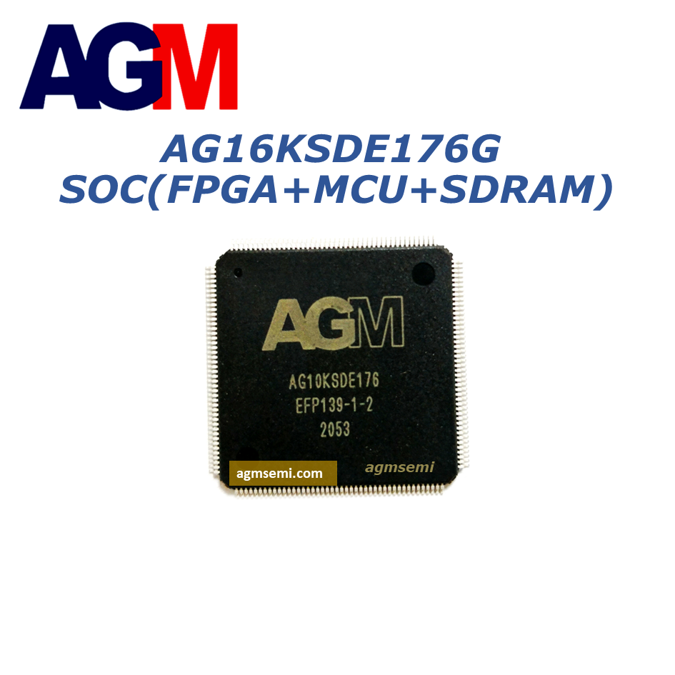
- AG16KSDE176G, QFP-176 package suppports 2-layer PCB(cost-down) design, with 139 user IOs.
AG16KDDF256 device is AG16K FPGA bonded with 128MBits 16-bit 200MHz DDR-SDRAM, FBGA-256 package supports 170 user IOs.
AGM SOC AG16KSDE176 (AG16K+MCU+SDRAM)
AG16K FPGA devices are targeted to high-volume, cost-sensitive, applications, enabling system designers to meet increasing performance requirements while lowering costs. The device AG16K offers supreme quality, stability, and exceptional pricing value.
Features
High-density architecture with 16K LEs
Up to 504Kbits of RAM space
Up to 56 18 x 18-bit embedded multipliers are each configurable as two independent 9 x 9-bit multipliers
Provides 4 PLLs per device provide clock multiplication and phase shifting
High-speed differential I/O standard support, including LVDS, RSDS, mini-LVDS, LVPECL
SSTL, SSTL-II IO standard, support DDR, DDR2
Single-ended I/O standard support, including 3.3V, 2.5V, 1.8V, and 1.5V LVCMOS and LVTTL
General package options, LQFP-144, -176 and FBGA-256
Two 12-bits SarADC (embedded temp sensor)
Flexible device configuration through JTAG and SPI interface
Support remote update, by "dual-boot" like implementation
Support on chip signal debugging
AG16KSDE176/AG16KSDF256/AG16KSDE176G devices are AG16K FPGA bonded with 64MBit 32-bit 166MHz SDRAM :
- AG16KSDE176, QFP-176 papckage suppports 2-layer PCB(cost-down) design. AG16KSDE176 is pin-to-pin compatible with AG10KSDE176.
- AG16KSDF256, FBGA-256 package supports 152 user IOs and 3 additional ADC IO.
- AG16KSDE176G, QFP-176 package suppports 2-layer PCB(cost-down) design, with 139 user IOs.
AG16KDDF256 device is AG16K FPGA bonded with 128MBits 16-bit 200MHz DDR-SDRAM, FBGA-256 package supports 170 user IOs.